Shenzhen Xindaxing ElectricTechnology Co., Ltd.
(Xing Da Electric Technology CO.,Ltd),whichhas been specializing in PCB/PCBA and Electronic components for manyyears.We can prvide a package ofservice:
- 1. PCB layout, PCB design;
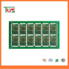
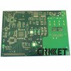
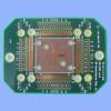
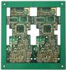
- 2: Make high difficulty PCB(1 to 38 layers)
- 3: Provide all Electronic components;
- 4: PCB assembly;
- 5: Write programs for clients;
- 6:PCBA/finished product Test.
- etc…
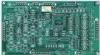
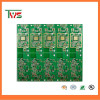
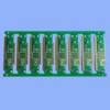
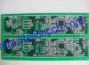
1.Specification for PCB&PCBA Manufacture:
Item | Specification |
Numbr of Layer | 1-38Layers |
Material | FR-4,FR2.Taconic,Rogers, CEM-1CEM-3,ceramic , crockery |
Metal-backedLaminate | |
Remarks | High Tg CCL IsAvailabe(Tg>=170ºC) |
Finish BoardThickness | 0.2mm-6.00mm(8mil-126mil) |
Minimun CoreThickness | 0.075mm(3mil) |
Copper Thickness | 1/2 oz min;12 ozmax |
Min.Trace Width & LineSpacing | 0.075mm/0.1mm(3mil/4mil) |
Min.Hole Diameter for CNCDriling | 0.1mm(4mil) |
Min.Hole Diameter forpunching | 0.9mm(35mil) |
Biggest panel size | 610mm*508mm |
Hole Positon | +/-0.075mm(3mil) CNCDriling |
Conductor Width(W) | +/-0.05mm(2mil)or |
+/-20% of originalartwork | |
Hole Diameter(H) | PTHL:+/-0.075mm(3mil) |
Non-PTHL:+/-0.05mm(2mil) | |
Outline Tolerance | +/-0.125mm(5mil) CNCRouting |
+/-0.15mm(6mil) byPunching | |
Warp & Twist | 0.70% |
InsulationResistance | 10Kohm-20Mohm |
Conductivity | <50ohm |
Test Voltage | 10-300V |
Panel Size | 110×100mm(min) |
660×600mm(max) | |
Layer-layermisregistration | 4layers:0.15mm(6mil)max |
6layers:0.25mm(10mil)max | |
Min.spacing between hole edge tocircuity pqttern of an inner layer | 0.25mm(10mil) |
Min.spacing between board oulinetocircuitry pattern of an inner layer | 0.25mm(10mil) |
Board thicknesstolerance | 4layers:+/-0.13mm(5mil) |
6layers:+/-0.15mm(6mil) | |
Impedance Control | +/-10% |
Different Impendance | +-/10% |
2.Quoterequirement
1).Many agile forms of cooperation(OEM ,ODM) arewelcome!
2).The detailed files(Gerber files andspecification);
3).Carbon PCB samples forus;
4).Carbon PCB Test method.