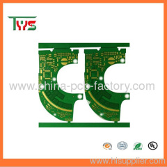


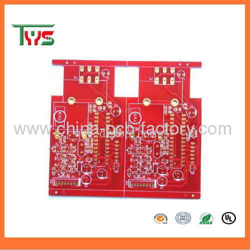
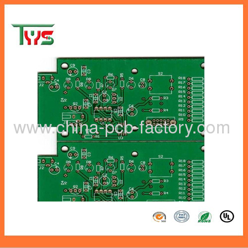
1.Single,double Layer PCB
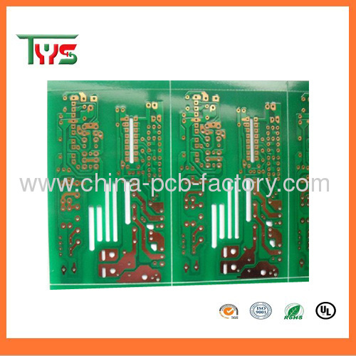
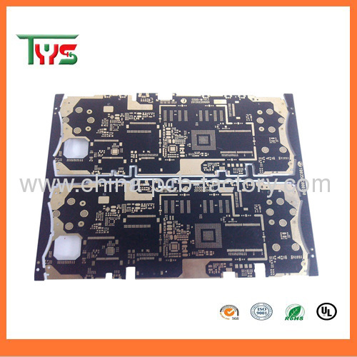
2.MultilayerPCB/HDI PCB (4L to 28Layers)
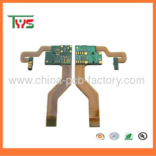
3.FlexiblePCB/Rigid Flexible PCB (single, double and 4Layers)
4.AluminumPCB
5.Componentssourcing and purchasing
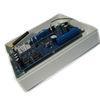
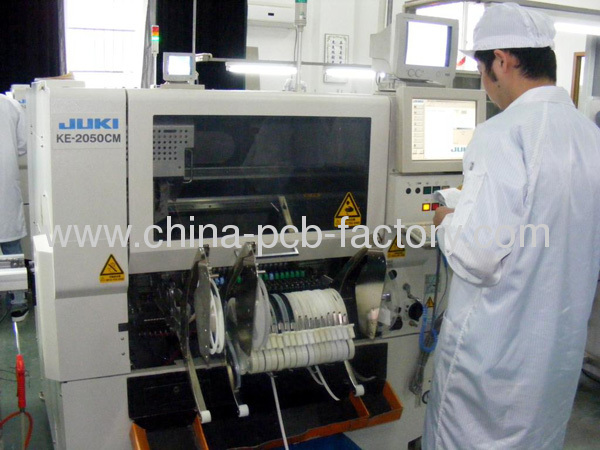
7.6.FinalPCB and FPC assembly: SMT & PTH & BGA
8.Customclearance for material importing and product exporting
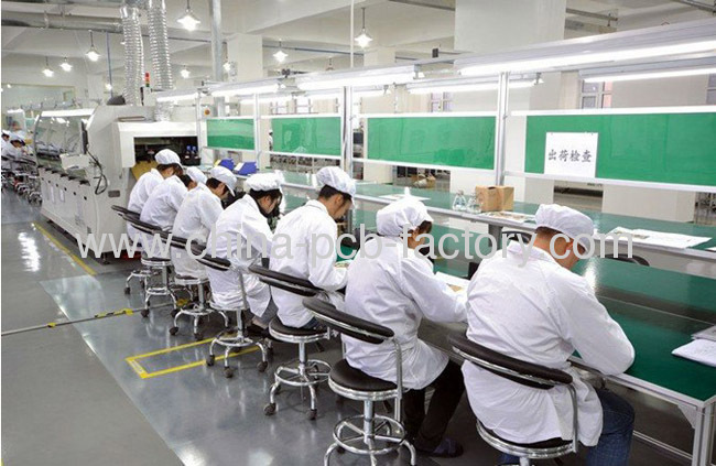
9.Test:AOI, In-Circuit Test (ICT), Functional Test (FCT)
Advantage
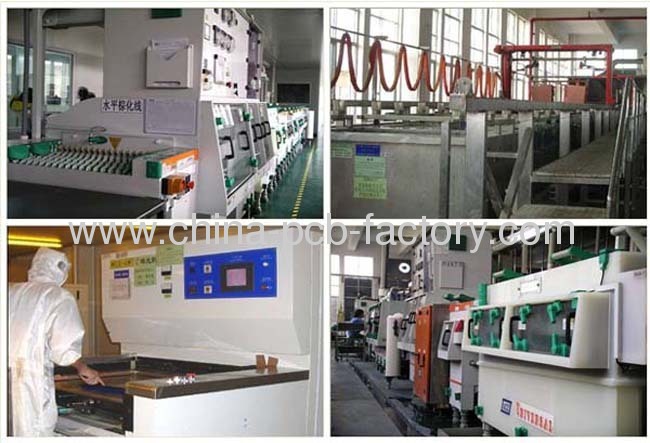
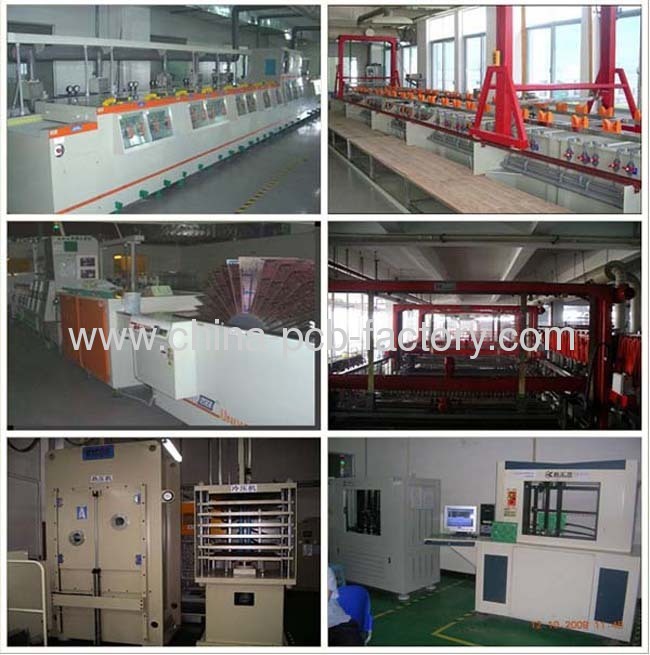
1.Automatedequipments to reduce the cost,
2.Our pricesare very competitive and quality is super
3.Fastaction/24hours quotation
4.Quickprototyping and production
5.Steadyand safe delivery to Russia by EMS, air or sea.
Major PCB parameters below canall be customised:
1) Layers, size,thickness
2) Base material :FR4,CEM3
3) Solder mask: Red,Green,Yellow,Blue or others
4) Characters:White(default)or others
5) Surface technique: Tinsoldering, plating gold, immersion gold,OSP
If you need to get a formal quoation,please providethe spec as below:
PCB files ingerber file, .pcb or .pcb doc formart ,specification and BOM
PCB Capacity
PCB Capacity
technologyproject | making ability and technologystandard |
Certificate | UL, RoHS, SGS |
Surface Finishing | Plating Nickel and immersion Gold, Hot Air (HASL), HASL Lead Free,OSP, Immersion Tin |
Max.panel size | 600mm*700mm |
Min.panel size | 5mm*5mm |
Boardwarpage | single side<=1.0% double side<=0.6% multi-layer<=0.6% |
Min.Thickness | 0.2mm±0.08mm |
Min.Line width | HASL board 0.07mm±20%(2mil±20%) |
Min.line space | immersion Gold 0.075mm±20%(2mil±20%) |
copperfoil to board sidespacing | 0.5mm |
hole sideto linesidespacing | 0.3mm |
Min hole size | 0.2mm |
copper thinckness of Hole | 20-35um |
Tooling hole tolerance | ±0.076mm |
Min.stamping round hole diameter | FR-4 board thinckness 1.0mm(40mil)under 1.0mm(40mil) |
Min.stamping round hole diameter | FR-4 board thinckness1.2-3.0mm(47mil-120mil)1.5mm(59mil) |
Min.stamping square hole specification | FR-4.CEM-3 board thinckness 1.0mm(40mil) under 0.8mm x0.8mm(31.5mil x 31.5mil) |
Min.stamping square hole specification | FR-4.CEM-3 board thinckness 1.2mm - 3.0mm(47mil-120mil) 1.0mm x1.0mm(40mil x 40mil) |
tracedeviation | ±0.076mm(±3mil) |
Molding size tolerancelimit | CNC milling profile ±0.15mm(±6mil); die profile±0.15mm(±6mil) |
V-CUT registration accuracy | ±0.2mm(±8mil) |
producttype | single sidedouble side multi-layer and flexibleboard |
Base Material | FR-4,CEM-1, CEM-3, High frequency, aluminium basedboard |
processthinckness | 0.2-3.5mm |
base materialcopperthinckness | 18um, 35um, 70um, 105 um |
Min.hold diameter | 0.2mm |
platingthinckness | plating gold Ni2.5-5um, Au0.05-0.10um |
platingthinckness | immersion gold Ni5-8um, Au0.08-0.12um |
platingthinckness | finger gold Ni2.5-5um, Au0.05-0.12um |
processability | 20000 square meters/month |
profileprocess | die CNC machine |
V-CUT horntolerance | ±5° |
V-CUT board materialthinckness | 0.6mm - 3.2mm (15.5mil - 129.58mil) |
Min.SMD space | 0.3mm (12mil) |
Min.component markingfont | 0.15mm (5.79mil) |
Min. single side solder annular width(production) | 0.15mm (5.79mil) |
Min. cross-hatchingpad | 0.076mm (0.3mil) |
Min.soldermask brigde | ±0.076mm(±3mil) |
Carbonink board making data | 1)1.0 high impedance control limit:20K±10% |
2)2.0 hardness:6H | |
3)3.0 can bear friction time:over 200000 |
PCBA assemblecapability
Quantity | Prototype&LowVolume PCB Assembly,from 1 Board to 250,is specialty,or up to1000 |
Typeof Assembly | SMT,Thru-hole |
SolderType | WaterSoluble Solder Paste,Leaded and Lead-Free |
Components | PassiveDown to 0201 size BGAand VFBGA LeadlessChip Carriers/CSP Double-sidedSMT Assembly FinePitch to 0.8mils BGARepair and Reball PartRemoval and Replacement |
BareBoard Size | Smallest:0.25*0.25inches Largest:20*20inches |
FileFormate | Billof Materials Gerberfiles Pick-N-Placefile |
Typesof Service | Turn-key,partialturn-key or consignment |
Componentpackaging | CutTape,Tube,Reels,Loose Parts |
TurnTime | Sameday service to 15 days service |
Testing | FlyingProbe Test,X-ray Inspection AOI Test |


LED DOUBLE SIDES PCB