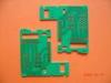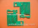


Heavy Copper 4 Layer Immersion Gold CEM 3 PCB Board with Green Solder Mask
High Tg PCB General Info
Tg means Glass Transition Temperature. As flammability of board is V-0 (UL 94-V0), so if the temperature exceeds designated Tg value, the board will changed from glassy state to rubbery state and then the function of board will be affected.
|
If working temperature of your product is higher than normal (130-140C), then have to use high Tg material which is > 170C. Here are some popular High Tg board raw material in market: |
S1170&S1000-2: SYL (Shengyi Technology);
Also there're a lot of different hi-tg material not listed here, different country, different company prefer using different material. Please view datasheet for each of them to choose most suitable material for you. If without special notice, normally we will use S1170 from SYL.
170Tg is also popular in LED industry, because heat dissipation of LED is higher than normal electronic components, and same structure of FR4 board is much cheaper than that of MCPCB. If working temperature is higher than 170/180C, such as 200C, 280C, or even higher, then you'd better use Ceramic boardwhich can go through -55~880C.
Please contact usfor more information about Hi Tg circuit board.
Heavy Copper PCB General Info
Heavy Copper Board does not have a set of definition per IPC. According to PCB industry, however, peopel generally use this name to identify a printed circuit board with copper conductors 3 oz/ft2 - 10 oz/ft2 in inner and/or outer layers. And Extreme heavy copper PCB refers to 20 oz/ft2 to 200 oz/ft2 printed circuit board
Heavy copper normally used for a various products but not limited to: high power distribution, heat dissipation, planar transformers, power convertors, and so on
Design Guide for Heavy Copper PCB
Typical conductor width/spacing/thickness tolerance is +/-20%, although tighter tolerance is achievable.
The minimum width and thickness of a heavy copper PCB conductor is determined primarily on the basis of the current carrying capacity required and the maximum permissible conductor temperature rise.
A circuit board trace, depending on its size and manufacturing process, may not be rectangular in shape. Heavy copper conductors can significantly add to the overall board thickness.
Additive (plating) processed are preferred to subtractive (etching) processes but are more expensive).
Capability of Heavy Copper PCB
Base material: FR4/Aluminum
Copper thickness: 4 OZ~6OZ
Outline: Routing, punching, V-Cut
Soldermask: White/Black/Blue/Green/Red Oil
Surface finishing: Immersion Gold, HASL, OSP
Description
1. Professional manufacturer of PCB specialized in single-sided PCB, double-sided PCB, multilayer PCB.
2. Material Type: FR4,non-halogen material ,Aluminium Base,Cooper Base,high frequency material ,Thick copper foil,94-V0(HB),PI Material,HIGH TG:SL S1000-2,ITEQ:IT180
3. Surface treatment: HAL,Immersion Gold,Immersion Tin,Immersion silver,Gold Finger,OSP,HAL(Immersion Gold,OSP,Immersion silver,Immersion Tin)+Gold Finger
Application
Products are applied to a wide range of High-tech industries such as: LED, telecommunication, computer application, lighting, game machine, industrial control, power, automobile and high-end consumer electronics, ect. By unremitting work and effort to the marketing, products exports to American, Canada, Europe counties, Africa and other Asia-pacific countries
Advantage
1. PCB factory directly
2. PCB Have the comprehensive quality control system
3. PCB good price
4. PCB quick turn delivery time from 48hours.
5. PCB certification(ISO/UL E354810/RoHS)
6. 8 years experience in exporting service
7. PCB is no MOQ/MOV.
8. PCB is high quality.Strict through theAOI(Automated Optical Inspection),QA/QC,fly porbe ,Etesting
|
|
High precision prototype |
PCB bulk production |
|
|
Max Layers |
1-28 layers |
1-14 layers |
|
|
MIN Line width(mil) |
3mil |
4mil |
|
|
MIN Line space(mil) |
3mil |
4mil |
|
|
Channel: madeinchina.hisupplier.com - hebei.hisupplier.com - ningbo.hisupplier.com Language Option:
العربية -
Nederlands-
Français-
Deutsch-
Italiano-
日本語-
한국의-
Português-
Pусский-
Español
IPR Protection Policy -
Terms of Use -
Privacy Policy -
Security Measures
Copyright © HiSupplier.com Online Inc. All Rights Reserved. | |||