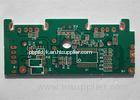


FR4 Custom Multi Layer PCB OSP White Silkscreen with UL for Power Bank
Quick Details:
1. Professional PCB manufacturer.
2. PCBA,OEM,ODM service are provided.
3. Gerber file needed.
4. Products are 100% E-tested.
5. Quality guarantee and professional after-sale service.
|
PRODUCT’S DETAILS |
|
|
Raw Material |
FR-4 (Tg 180 available) |
|
Layer Count |
8-Layer |
|
Board Thickness |
1.6mm |
|
Copper Thickness |
2.0oz |
|
Surface Finish |
ENIG(Electroless Nickel Immersion Gold) |
|
Solder Mask |
Green |
|
Silkscreen |
White |
|
Min. Trace Width/Spacing |
0.075/0.075mm |
|
Min. Hole Size |
0.25mm |
|
Hole Wall Copper Thickness |
≥20μm |
|
Measurement |
300×400mm |
|
Packaging |
Inner: Vacuum-packed in soft plastic bales |
|
Application |
Communication,automobile,cell,computer,medical |
|
Advantage |
Competitive Price,Fast Delivery,OEM&ODM,Free Samples, |
|
Special Requirements |
Buried And Blind Via, Impedance Control, Via Plug, |
|
Certification |
UL,ISO9001:2008,ROHS,REACH,SGS,HALOGEN-FREE |
|
PRODUCTION CAPABILITY OF PCB |
||
|
Process Engineering |
Items |
Manufacturing Capability |
|
Laminate |
Thickness |
0.23.2mm |
|
Production Type |
Layer Count |
2L-16L |
|
Cut Lamination |
Max. Working Panel size |
1000×1200mm |
|
Inner Layer |
Internal Core Thickness |
0.12.0mm |
|
Internal width/spacing |
Min: 4/4mil |
|
|
Internal Copper Thickness |
1.0~3.0oz |
|
|
Dimension |
Board Thickness Tolerance |
±10% |
|
Interlayer Alignment |
±3mil |
|
|
Drilling |
Manufacture Panel Size |
Max: 650×560mm |
|
Drilling Diameter |
0.25mm |
|
|
Hole Diameter Tolerance |
±0.05mm |
|
|
Hole Position Tolerance |
±0.076mm |
|
|
Min.Annular Ring |
0.05mm |
|
|
PTH+Panel Plating |
Hole Wall copper Thickness |
20um |
|
Uniformity |
90% |
|
|
Outer Layer |
Track Width |
Min: 0.08mm |
|
Track Spacing |
Min: 0.08mm |
|
|
Pattern Plating |
Finished Copper Thickness |
Didn't find what you're looking for?
Post Buying Lead or
contact our customer service specialist for help!
About HiSupplierUser GuideFeatured Partners:
Follow Us:


Channel: madeinchina.hisupplier.com - hebei.hisupplier.com - ningbo.hisupplier.com Language Option: العربية - Nederlands- Français- Deutsch- Italiano- 日本語- 한국의- Português- Pусский- Español IPR Protection Policy - Terms of Use - Privacy Policy - Security Measures Copyright © HiSupplier.com Online Inc. All Rights Reserved. 
|