
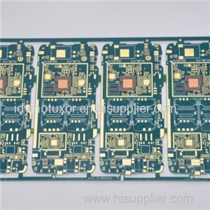
what's HDI pcb board ?HDI is High Density interconnect (High Density Interconnector) abbreviation, is one of the production of printed circuit board, using micro buried blind hole technology of a circuit board connect to more high density circuit line.PCB board SpecificationsPcb thickness:1.6mmLayer account:6LSurface finished:immersion gold+blind and bury via hole;Line width&space3/3milsFinished copper:1ozSolder mask:blue;Material:FR4.Certificates:CQC,ISO.TS16949,SGS,ISO9001,UL,ISO.14001,ROHSDelivery time:sample 3-5days,mass production:12-15days;Package details:vacuum pcb,inside bubble all inside,cartoon,ties outside strengthening;KDPCB Advantages1--never set any moq for every pcb board order;2--shortest response for all clients need;3--reasonable competitive price with high quality;4--support "one-stop"service for part of clients;5--shortest delivery time on pcb board production;6--"5S"and ISO.TS16949 quality system control manufacture;7--professional,high communication,trustworthy;8--all kinds of pcb board manufacture are acceptable;9--TNT/UPS/DHL/FEDEX/special shipping agency support with lower price;HDI pcb advantage1)can reduce the cost of PCB: after more than eight layer plate with HDI manufacturing, the cost will be lower than traditional pcb board manufacture;2)Increase the line density: interconnection of traditional circuit board and parts;3)For the use of advanced packaging technology;4)Have a better performance and accuracy of the signal;5)Reliability is better;6)Can improve thermal properties;7)Can improve the rf interference/electromagnetic interference/(RFI/EMI/ESD), electrostatic discharge;8)To increase design efficiency;9)Ability to meet the density constraints of lines and pads on a typical design without increasing the layer count or board size;kdpcb has years of experience in manufacturing HDI PCBs with Blind & Buried Vias. Both our engineers and production facility are equipped to handle the intricacy this technique requires, with very high accuracy.While this technique is more costly, we have seen savings through the reduction of layers or board size. This trend is becoming more and more popular within the PCB industry.kdpcb material vendors is only the famous brand manufacturers such as KB group/ITEQ/ROGERS and others;With us, you receive unparalleled technical expertise support for HDI pcb manufacture;we strive for our customers to feel that our service is so unique and valuable that they would want to work with us forever.We understand that 1)you want solutions support not always make trouble to you ,2) you want what you need and not what a boardhouse wants to sell you.application fieldMobile phones,digital (photo) camera,MP3,MP4,notebook computers,automotive electronics and other digital products;3G mobile phone, advanced digital video camera, IC carrier board;others electronics.
Home >
Electronic & Electrical
>
6 Layer Microvia Pcb Board With 3oz Inner Copper
6 Layer Microvia Pcb Board With 3oz Inner Copper
Trade on HiSupplier, Worry Free Guarantee
•Trading safety, secure your money, lower the risk, protect both buyers and suppliers
•HiSupplier is a Chinese multinational company in U.S, it helps to coordination and order landing.
- Product Details
- Company Profile
- Product Reviews

Didn't find what you're looking for?
Post Buying Lead or
contact our customer service specialist for help!


