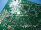
GPS Logger 10 Layer BGA PCB High Tg FR4 1.6mm 1oz With Green Mask
PCB parameters
| PCB SIZE | 245 x 221mm=1PCS |
| BOARD TYPE | |
| Number of Layers | Multilayer PCB, 10 Layer PCB |
| Surface Mount Components | YES |
| Through Hole Components | YES |
| LAYER STACKUP | copper ------- 35um(1oz)+plate TOP Signal |
| 4mil prepreg | |
| copper ------- 18um(0.5oz) GND Plane | |
| 5mil FR-4 | |
| copper ------- 18um(0.5oz) SIG1 | |
| 5mil prepreg | |
| copper ------- 18um(0.5oz) SIG2 | |
| 5mil FR-4 | |
| copper ------- 18um(0.5oz) PWR Plane | |
| 13mil prepreg | |
| copper ------- 18um(0.5oz) GND Plane | |
| 5mil FR-4 | |
| copper ------- 18um(0.5oz) SIG3 | |
| 5mil prepreg | |
| copper ------- 35um(1oz) SIG4 | |
| 5mil FR-4 | |
| copper ------- 35um(1oz) GND Plane | |
| 4mil prepreg | |
| copper ------- 35um(1oz)+plate BOT Signal | |
| TECHNOLOGY | |
| Minimum Trace and Space: | 4mil/4mil |
| Minmum / Maximum Holes: | 0.25/9.0mm |
| Number of Different Holes: | 19 |
| Number of Drill Holes: | 5112 |
| Number of Milled Slots: | 2 |
| Number of Internal Cutouts: | 0 |
| Impedance Control | Differential pairs impedance control and Single trace impedance control |
| BOARD MATERIAL | |
| Glass Epoxy: | FR-4, ITEQ IT-180 TG>170, er<5.4 |
| Final foil external: | 1.5oz |
| Final foil internal: | 0.5oz |
| Final height of PCB: | 1.6mm ±0.16 |
| PLATING AND COATING | |
| Surface Finish | Immersion Gold (20.1%) 2µ" over 100µ" nickel |
| Solder Mask Apply To: | Top and Bottom, 12micon Minimum. |
| Solder Mask Color: | Green, LP-4G G-05, Nanya supplied |
| Solder Mask Type: | LPSM |
| CONTOUR/CUTTING | Routing |
| MARKING | |
| Side of Component Legend | TOP |
| Colour of Component Legend | White, S-380W, Taiyo Supplied. |
| Manufacturer Name or Logo: | Marked on the board in a conductor and leged FREE AREA |
| VIA | Plated Through Hole(PTH), Ball grid array (BGA) package with via capped. |
| FLAMIBILITY RATING | UL 94-V0 Approval MIN. |
| DIMENSION TOLERANCE | |
| Outline dimension: | 0.0059" (0.15mm) |
| Board plating: | 0.0030" (0.076mm) |
| Drill tolerance: | 0.002" (0.05mm) |
| TEST | 100% Electrical Test prior shipment |
| APPLICATION: | Gps Logger |
| TYPE OF ARTWORK TO BE SUPPLIED | email file, Gerber RS-274-X, PCBDOC etc |
| SERVICE AREA | Worldwide, Globally. |
Advantages
a) FR-4 epoxy glass. UL94V0. Lead-Free Assembly Compatible, RoHS compliant and suitable for high thermal reliability needs, and Lead free assemblies with a maximum reflow temperature of 260
b) Immersion gold surface finish. Excellent surface planarity, particularly helpful for PCBs with BGA packages or even CSP mounted components to reduce failure rate during assembly and soldering.
c) No MOQ, low cost for small quantity prototypes and samples.
d) ISO certified PCB manufacturing factory.
e) DDU Door to door shipment with competitive shipping cost.
More Applications in Electronics
Lan Switch
Gps Tracker For Car
Step Up Transformer
Usb Wireless
12 Volt Battery Charger
Wireless Speaker System
PCB knowledge: PCB Production Process
1. Contact PCB fabricator
Contact your satisfied vendor such as Bicheng. You’re registered and will be quoted for you. Place your order and follow up the production schedule.
2. Material cutting
Purpose: According to the requirement from engineering data, cut the large plate which is in compliance with the requirement into small pieces of production board piece to meet customer requirements of the small sheet.
3. Drill
Purpose: According to the requirement from engineering data, drill all the holes.
4. Copper deposition
Purpose: Copper deposition is a thin copper deposit on the wall of the insulating hole by chemical method
5. Pattern transfer
Purpose: Pattern transfer is the transfer of image production on the film to the board
6. Pattern plating
Purpose: Pattern electroplating is a layer of copper or gold over nickel or tin that requires a thickness plated on the exposed copper of the pattern graphic or on the hole wall.
7. Film stripping
Purpose: The NaOH solution is used to strip the anti-plating film to expose the non-pattern circuit layer.
8. Etching
Purpose: Etching is to etch off the non-circuit parts of the copper layer by chemical reaction method
9. Solder Mask
Purpose: Solder mask is transferring the solder mask film graphics to the board to protect the track and prevent the track from the effect of tin welding during assembly.
1