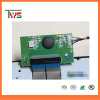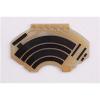


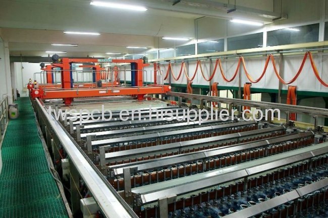
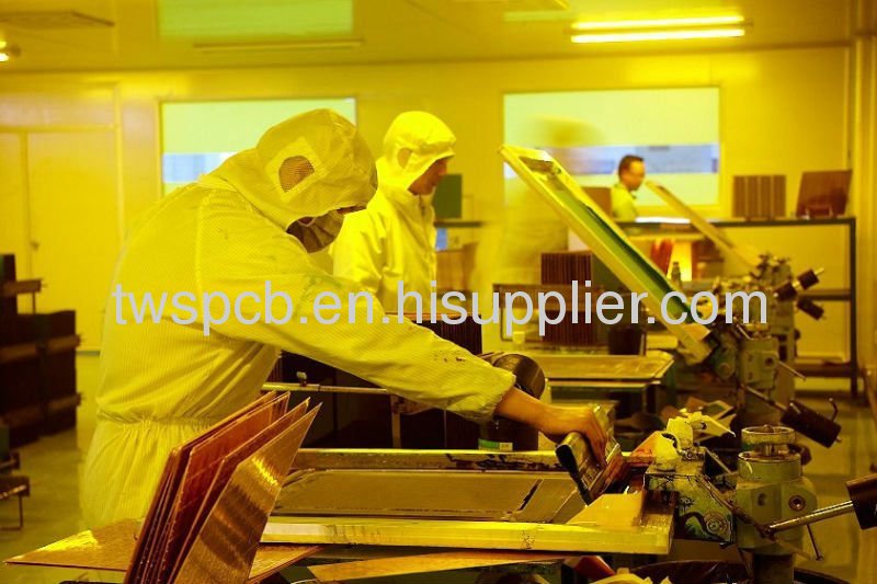
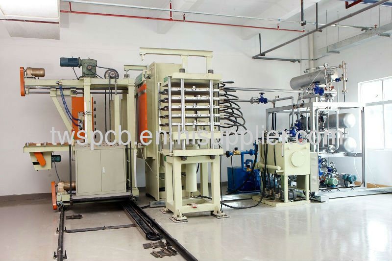
Advanced ProductionEquipment
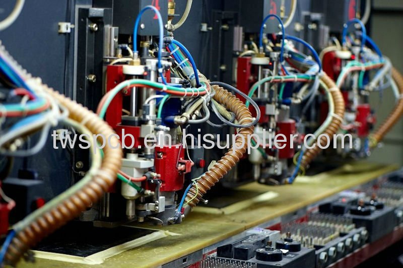
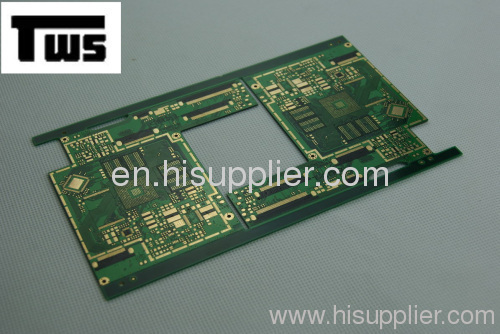
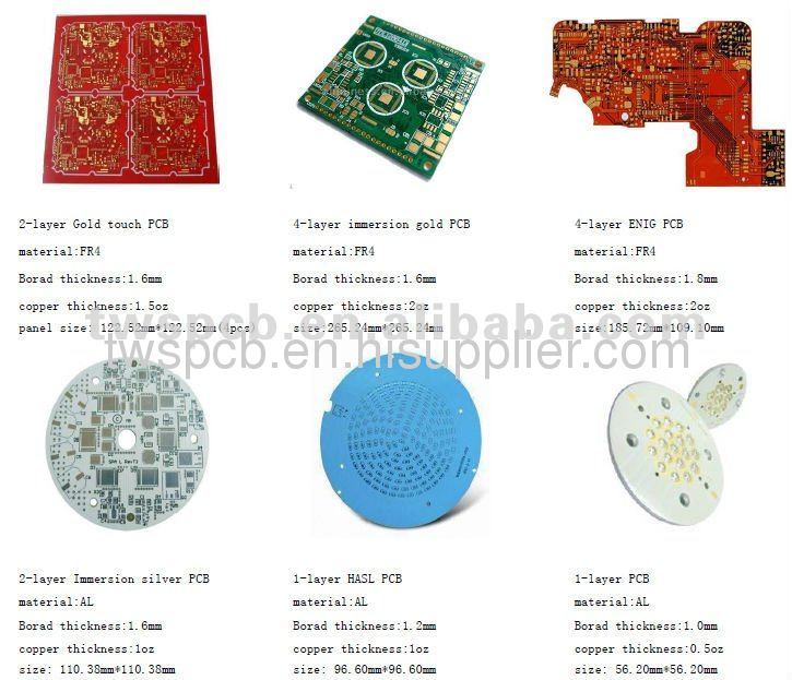
Product HighQuality Perfect
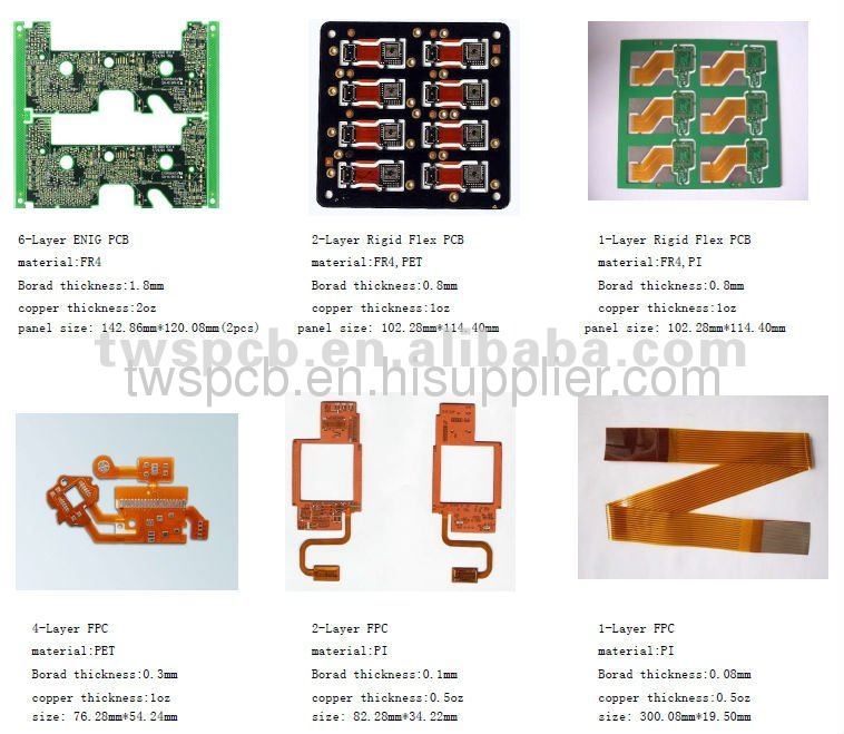
Meet your need is ourgreatest pursuit .If you are looking for a pcb board manufacturerinchina,Pleasegive us your files ofpcb for a quote (Gerberfiles and specification),I will reply email in 3hours. Youalso cancontact usby .
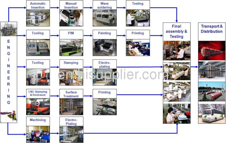
1.Advanced production lines andprofessional staff.
2.Honesty credibility in china'stop.
3.Competest price but highquality.
4. One-stopservice.
5.Delivery ontime.
NO | Item | Craft Capacity |
1 | Layer | 1-30 Layers |
2 | Base Material for PCB | FR4, CEM-1, TACONIC, Aluminium, High Tg Material, High Frequence ROGERS ,TEFLON, ARLON, Halogen-free Material |
3 | Rang of finish baords Thickness | 0.21-7.0mm |
4 | Max size of finish board | 900MM*900MM |
5 | Minimum Linewidth | 3mil (0.075mm) |
6 | Minimum Line space | 3mil (0.075mm) |
7 | Min space between pad to pad | 3mil (0.075mm) |
8 | Minimum hole diameter | 0.10 mm |
9 | Min bonding pad diameter | 10mil |
10 | Max proportion of drilling hole and board thickness | 1:12.5 |
11 | Minimum linewidth of Idents | 4mil |
12 | Min Height of Idents | 25mil |
13 | Finishing Treatment | HASL (Tin-Lead Free), ENIG(Immersion Gold), Immersion Silver , Gold Plating (Flash Gold), OSP, etc. |
14 | Soldermask | Green, White, Red, Yellow, Black, Blue, transparent photosensitive soldermask, Strippable soldermask. |
15 | Minimun thickness of soldermask | 10um |
16 | Color of silk-screen | White, Black, Yellow ect. |
17 | E-Testing | 100% E-Testing (High Voltage Testing); Flying Probe Testing |
18 | Other test | ImpedanceTesting,Resistance Testing, Microsection etc., |
19 | Date file format | GERBER FILE and DRILLING FILE, PROTEL SERIES, PADS2000 SERIES, Powerpcb SERIES, ODB++ |
20 | Special technological requirement | Blind & Buried Vias and High Thickness copper |
21 | Thickness of Copper | 0.5-14oz (18-490um) |
Specifications
1.Shenzhen PCBA assembly service
2.MilitarySpecifications
3.''Green'' Product
4.No MOQ
5.ISO9001/TS16949/IPC/ROHS/UL
2.MilitarySpecifications
3.''Green'' Product
4.No MOQ
5.ISO9001/TS16949/IPC/ROHS/UL
Packaging& Delivery Detail:
Packingdetail: Inner packing: Vaccum packing / Plastic bag / Outer packing:Standard carton packing
DeliveryDetail:
sample:Double-layer:1-3 days; Multi-layer:2-5 days
mass:Double-layer:2-7 days;Multi-layer:5-7days
Paymentterm:
Major PCB parameters below canall be customised:
1) Layers, size,thickness
2) Base material :FR4,CEM3
3) Solder mask: Red,Green,Yellow,Blue or others
4) Characters:White(default)or others
5) Surface technique: Tinsoldering, plating gold, immersion gold,OSP
If you need to get a formal quoation,please providethe spec as below:
PCB files ingerber file, .pcb or .pcb doc formart ,specification and BOM