OEM/ODM original printed circuit board with CE/Rohs/SGS

Price: 0.1~0.5 USD
Trade Term: FOB
Payment Terms: T/T,WU,
skype
Trade on HiSupplier, Worry Free Guarantee
Trading safety, secure your money, lower the risk, protect both buyers and suppliers
HiSupplier is a Chinese multinational company in U.S, it helps to coordination and order landing.
More ›
  • Product Details
  • Company Profile
  • Product Reviews
Basic Info.
  • Number of Layers: 4-Layer 
  • Brand Name: tws 
  • Base Material: fr4 
  • Copper Thickness: 1oz 
  • Board Thickness: 1.6mm 
  • Min. Hole Size: 0.15mm 
  • Min. Line Width: 0.2mm 
  • Min. Line Spacing: 0.2mm 
  • Surface finishing: HASL&ENIG 
  • Solder mask: Green/Blue/Black/White/Yellow/Red etc 
  • Max size of finish board: 9200*900mm 
  • Certification: UL/SGS/ROHS 
  • Controlled impedance: ±5% 
  • Warp&Twist: 0.7% 
  • Rang of finish boards thickness: 0.21~7.0mm 
  • Layer count: 1~28 
  • OEM/ODM: One-stop service 
  • PCB standard: IPC-A-610D 
  • Model No.: TWS 
  • Place of Origin: Guangdong  
  • Min.Order: 5 Piece/Pieces
  • Means of Transport: Ocean, Air, Land
Supply Capacity
  • Production Capacity: 300000 Square Meter/Square Meters / Month
  • Packing:vacuum package+carton box
  • Delivery Date: 10-15 working days for mass pcb order.
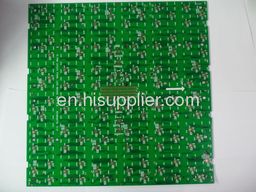
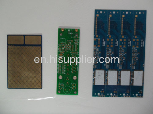
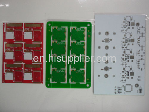
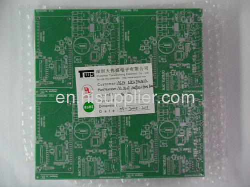
Original printed circuit board
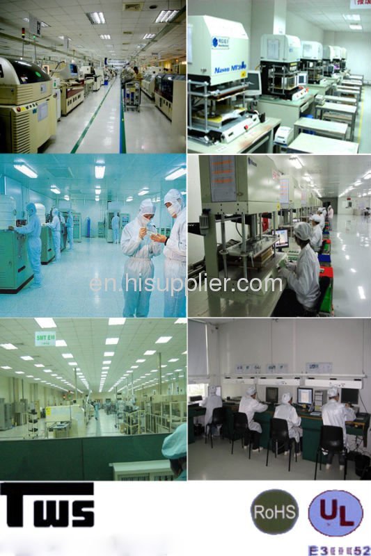
PCB experience10 years
PCB certificate:ISO,UL and ROHS
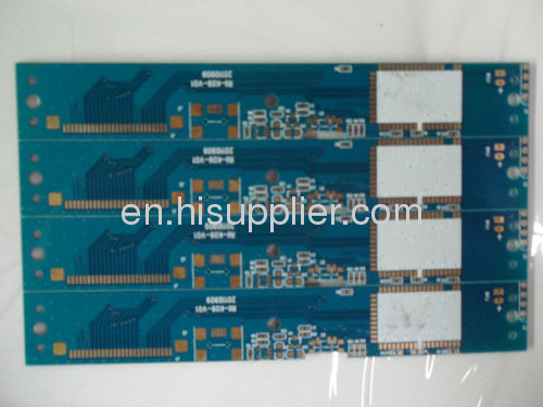
Red solder,1.6mm thick
PCB Board/Printed Circuit Board Manufacturer
1.We have 10 years experience in pcb field to serve your needs
2.Competitive pcb price with high quality
3.Excellent service and prompt delivery
4.Our pcb get ISO and UL Certificates and meet ROHS standard
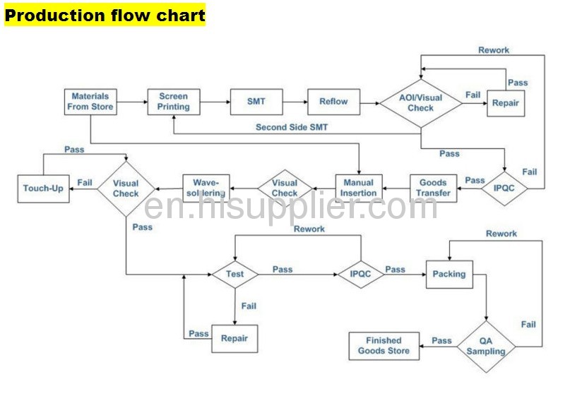

Testing Items
  • 100% Electrical Test
  • 100% Visual Inspection (including warp & twist check)
  • Dimensional Inspection (finished hole sizes, pcb profiles, etc)
  • Microsection
  • Solderability Test (245±5ºC; 3-5 sec)
  • Thermal Test (288±5ºC; 10 sec. inspect delamination, etc)
  • Tape Test (adhesion test)
  • Peel Test (conductor peel strength)
  • Impedance Test
  • Ionic Contamination Test
Our  PCB Technical capabilities
NO
ITEM
Our PCB Technical capabilities
1
Layers
2-20 layers
2
Max. Board size
2000×610mm
3
Min. board Thickness
2-layer 0.15mm
4-layer 0.38mm
6-layer 0.55mm
8-layer 0.80mm
10-layer 1.0mm
4
Min. line Width/Space
0.075mm(3mil)
5
Max. Copper thickness
6OZ
6
Min. S/M Pitch
0.075mm(3mil)
7
Min. hole size
0.1mm(4mil)
8
Hole dia. Tolerance (PTH)
±0.05mm(2mil)
9
Hole dia. Tolerance (NPTH)
+0/-0.05mm(2mil)
10
Hole position deviation
±0.05mm(2mil)
11
Outline tolerance
±0.10mm(4mil)
12
Twist & Bent
0.75%
13
Insulation Resistance
>1012 Ω Normal
14
Electric strength
>1.3kv/mm
15
S/M abrasion
>6H
16
Thermal stress
288°C 20Sec
17
Test Voltage
50-300V
18
Min. blind/buried via
0.15mm (6mil)
19
Surface Finished
HAL, ENIG, ImAg, Imsn OSP, Plating AG, Plating gold
20
Materials
FR4,H-G,Teflon,Rogers,Ceramics,Aluminium, Copper base

OEM/ODM original printed circuit board with CE/Rohs/SGS


Send message to this supplier
Ms. Grace
Tel: 86-755-29087997
Mobile: 13510820959
Enter between 20 to 3,000 chatacters.
Contact Method
Shenzhen Tianweisheng Electronic Co., Ltd.
4F, No. 48 Bldg., Gongle Ind. Zone, Xixiang Street, Bao' an District, Shenzhen, Guangdong, China (Mainland)
Fax: 86-755-29667579
Didn't find what you're looking for? Post Buying Lead or contact our customer service specialist for help!
Buyer Help Center