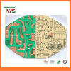
SpecificationforPCB&PCBA Manufacture:
Item | Specification |
Numbr of Layer | 1-38Layers |
Material | FR-4,FR2.Taconic,Rogers, CEM-1 CEM-3,ceramic ,crockery |
Metal-backed Laminate | |
Remarks | High Tg CCL IsAvailabe(Tg>=170ºC) |
Finish Board Thickness | 0.2mm-6.00mm(8mil-126mil) |
Minimun Core Thickness | 0.075mm(3mil) |
Copper Thickness | 1/2 oz min;12 oz max |
Min.Trace Width & LineSpacing | 0.075mm/0.1mm(3mil/4mil) |
Min.Hole Diameter for CNCDriling | 0.1mm(4mil) |
Min.Hole Diameter for punching | 0.9mm(35mil) |
Biggest panel size | 610mm*508mm |
Hole Positon | +/-0.075mm(3mil) CNCDriling |
Conductor Width(W) | +/-0.05mm(2mil)or |
+/-20% of originalartwork | |
Hole Diameter(H) | PTH L:+/-0.075mm(3mil) |
Non-PTH L:+/-0.05mm(2mil) | |
Outline Tolerance | +/-0.125mm(5mil) CNCRouting |
+/-0.15mm(6mil) byPunching | |
Warp & Twist | 0.70% |
Insulation Resistance | 10Kohm-20Mohm |
Conductivity | <50ohm |
Test Voltage | 10-300V |
Panel Size | 110×100mm(min) |
660×600mm(max) | |
Layer-layer misregistration | 4 layers:0.15mm(6mil)max |
6 layers:0.25mm(10mil)max | |
Min.spacing between hole edge to circuitypqttern of an inner layer | 0.25mm(10mil) |
Min.spacing between board oulineto circuitrypattern of an inner layer | 0.25mm(10mil) |
Board thickness tolerance | 4 layers:+/-0.13mm(5mil) |
6 layers:+/-0.15mm(6mil) | |
Impedance Control | +/-10% |
Different Impendance | +-/10% |
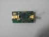
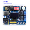
Details for PCBAssembly
1.Technical
1).Professional surfacemounting and through hole soldering technology;
2).Varioussizes,like 1206,0805,0603 components SMT technology;
3).ICT(InCircuit Test),FCT(Functional Circuit Test) technology;
4).Nitrogengas reflow soldering technology for SMT;
5).Highstandard SMT&Solder Assembly line;
6).Highdensity interconnected board placement technology capacity.
2.Quoterequirement
1).The detailed files(Gerberfiles,specification andBOM);
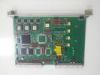
2).Clearpictures of PCBA or samples for us;
3).PCBATest method.