


Quick Details
| Place of Origin: | Guangdong China (Mainland) | Brand Name: | POE | Model Number: | POE-666 |
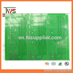
| Number of Layers: | 4-Layer | Base Material: | FR4 | Copper Thickness: | 70UM |
| Board Thickness: | 1.2MM | Min. Hole Size: | 0.15MM | Min. Line Width: | 0.2MM |
| Min. Line Spacing: | 0.2MM | Surface Finishing: | Immersion gold | Color: | Red |
Packaging & Delivery
| Packaging Detail: | CNC ESD |
| Delivery Detail: | 15days |
Specifications
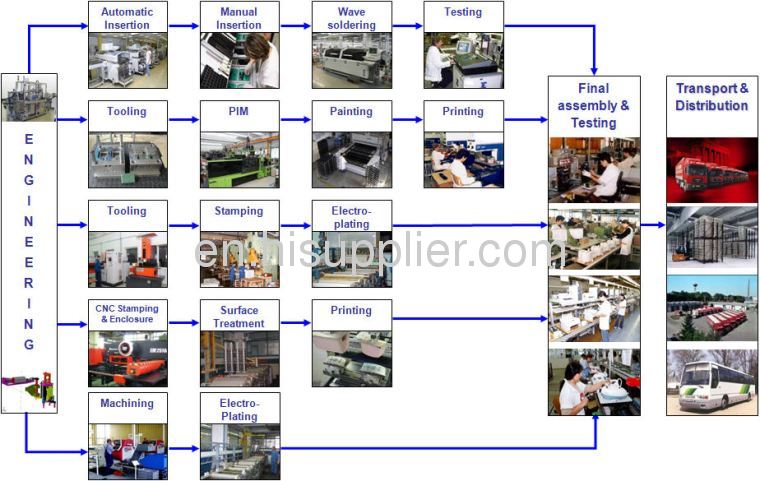
1.PCB printed circuit board fabrication
2.Good quality& service
3.Mass production & fast delivery
4.Low price
2.Good quality& service
3.Mass production & fast delivery
4.Low price
Detailed ProductDescription
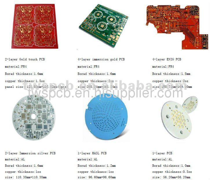
1.PDS PCB printed circuitboards
2.High quality high precision PCBassembly Prototype and MP
2.High quality high precision PCBassembly Prototype and MP
3.CNC package for bare PCB and ESD package forPCBA aasemble with POE box Package
Layer: 4Layer
Material: FR4
Thickness: 1.2mm
Copper thickness: Inner 2oz, outer2oz
Mini Hole: 0.15mm
Mini Width/space: 0.15mm/0.2mm
Testing points:5500
Solder Mask: LPI Red
Sickscreen: White
Function:PDS products
Finish: Immersion Gold
WELCOME TOPOE
1. POE PCB ManufactureCapability
Item | Capability | |
1.Base Material | FR-4 / High TG FR-4 / Lead free Materials (ROHSCompliant) / Halogen Free material /CEM-3/CEM-1//PTFE/ROGERS/ARLON/TACONIC | |
2.Layers | 1-28 | |
3.Finised inner/outer copper thickness | 1-6OZ | |
4.Finished board thickness | 0.2-7.0mm | |
Tolerance | Board thickness≤1.0mm: +/-0.1mm 1<Board thickness≤2.0mm: +/-10% Board thickness>2.0mm: +/-8% | |
5.Max panel size | ≤2sidesPCB: 600*1500mm Multilayer PCB: 500*1200mm | |
6.Min conductor line width/spacing | Inner layers: ≥3/3mil Outer layers: ≥3.5/3.5mil | |
7.Min hole size | Mechanical hole: 0.15mm Laser hole: 0.1mm | |
Drilling precision: first drilling | First drilling: 1mil Second drilling: 4mil | |
8.Warpage | Board thickness≤0.79mm: β≤1.0% 0.80≤Board thickness≤2.4mm: β≤0.7% Board thickness≥2.5mm: β≤0.5% | |
9.Controlled Impedance | +/-5% | |
10. Aspect Ratio | 15:1 | |
11.Min welding ring | 4mil | |
12.Min solder mask bridge | ≥0.08mm | |
13.Plugging vias capability | 0.2-0.8mm | |
14. Hole tolerance | PTH: +/-3mil NPTH: +/-2mil | |
15.Outline profile | Rout/ V-cut/ Bridge/ Stamp hole | |
16.Surface treatment | OSP: 0.5-0.5um HASL: 2-40um Lead free HASL: 2-40um ENIG: Au 1-10U'' ENEPIG: PB 2-5U''/ Au 1-8U'' Immersion Tin:0.8-1.2um Immersion silver: 0.1-1.2um Peelable blue mask Carbon ink Gold plating: Au 1-150U'' | |
17. E-testing pass percent | 97% pass for the firsttime,+/-2%(tolerance) | |
FQC-Physical Lab: Reliabilitytests | ||
18.Certificate | ROHSUL:E327776ISO9001:2008IPC SGS | |
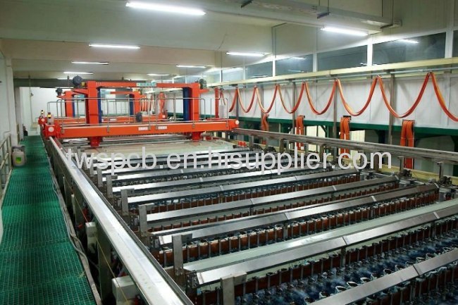
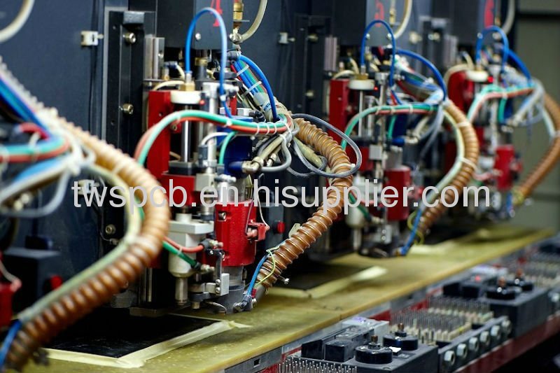
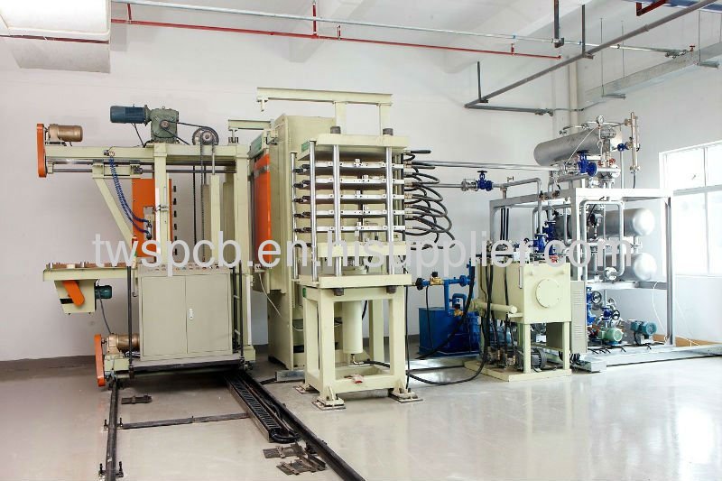
Our equipments | ||
1.Drilling workshop | 4 drilling bits of drilling machine: 4 sets 2 drilling bits of drilling machine: 2sets | |
2. photo plotting workshop | Israel "ORBOTECH" Photo Plotters | |
3.AOI | AOI machine | |
4.IPQC | "OXFORD" CMI 700 Copper ThicknessTester | |
5.Impedance test | USA "Tektronix" DSA 8200 ImpedanceTester | |
6.Outline workshop | CNC routing machine: 7 sets angle-cutting machine V-cut machine | |
7.Testing Workshop | Surpass X-600: 2sets WTD FT-2808: 5sets WTD HV300: 1set | |
8.X-ray | X-ray machine | |
Acceptable file format | ||
GERBER file, PROTEL series, PADS series, POWERPCB series, AutoCAD series. | ||
…………… …………… ………………
Product HighQuality Perfect

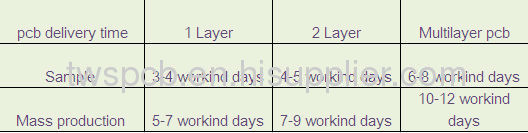
Our deliverytime:
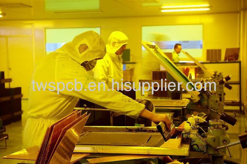
1.About Factory:
Experience: we have 20 years experinecsin circuit board manufacturing,with 50 employees and 60 excellent engineers,covering an area of 13000 square meters.Monthly capability is more than 5000square meters, 4500 types/month. we cooperate with some well-known enterprises,such as Panasonic, HP,Honeywell and so on.
2.Good after sales service:
anything wrong happening in our products willbe solved within 2 hours. we always offer relative technical support/consultant.Quick response. all your inquiry will be replied within 24 hours.
3.Ourproducts and service are sold well in North America,West Europe, Japan,Singpore, Malaysia and other countries.


Meet your need is ourgreatest pursuit .If you are looking for a pcb board manufacturerinchina,Pleasegive us your files ofpcb for a quote (Gerberfiles and specification),I will reply email in 3hours. Youalso cancontact usby .
1.Advanced production lines andprofessional staff.
2.Honesty credibility in china'stop.
3.Competest price but highquality.
4. One-stopservice.
5.Delivery ontime.