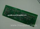


Gold Finish Double Sided PCB 2 Layer Printed Circuit Board for Electronics
S/S and 2 Layers PCB General Information
"S/S PCB" full name is "Single Sided PCB", or you can name it as Single Layer PCB, or 1L PCB. There's no only one copper trace on the board, SMD components on one side (through hole components at the other side), no PTH (plated through hole) or via, only has NPTH (no-plated through hole), or location hole.
It is the cheapest type of board, and used in very simple board. In order to get a cheaper price, sometimes people will use CEM-1, CEM-3 instead of FR4, to make the circuit board. Also most PCB raw material vendor don't make 1 Layer FR4, but 2L one, so one copper trace need to be etched away in PCB fabrication.
There's another conventional board "2L PCB" which has 2 copper trace, and also named as "Double Sided PCB" (D/S PCB), and PTH (Via) is a must, but it still doesn't has Buried or Blind hole. Components can be assembled on both top and bottom side, so you don't need to worry about where to put components on the board, and not need to use through hole components which is always expensive than SMD one.
Currently this is one of the most popular types of PCB on the Earth, and we can provide 24 hours quick-turn service for them.
Capability
High precision prototype | PCB bulk production | ||
Max Layers | 1-28 layers | 1-14 layers | |
MIN Line width(mil) | 3mil | 4mil | |
MIN Line space(mil) | 3mil | 4mil | |
Min via (mechanical drilling) | Board thickness≤1.2mm | 0.15mm | 0.2mm |
Board thickness≤2.5mm | 0.2mm | 0.3mm | |
Board thickness2.5mm | Aspect Ration≤13:1 | Aspect Ration≤13:1 | |
Aspect Ration | Aspect Ration≤13:1 | Aspect Ration≤13:1 | |
Board thickness | MAX | 8mm | 7mm |
MIN | 2 layers:0.2mm;4 layers:0.35mm;6 layers:0.55mm;8 layers:0.7mm;10 layers:0.9mm | 2 layers:0.2mm;4 layers:0.4mm;6 layers:0.6mm;8layers:0.8mm | |
MAX Board size | 610*1200mm | 610*1200mm | |
Max copper thickness | 0.5-6oz | 0.5-6oz | |
Immersion Gold/ | Immersion Gold:Au,1—8u” | ||
Hole copper thick | 25um 1mil | 25um 1mil | |
Tolerance | Board thickness | Board thickness≤1.0mm:+/-0.1mm | Board thickness≤1.0mm:+/-0.1mm |
Outline Tolerance | ≤100mm:+/-0.1mm | ≤100mm:+/-0.13mm | |
Impedance | ±10% | ±10% | |
MIN Solder mask bridge | 0.08mm | 0.10mm | |
Plugging Vias capability | 0.25mm--0.60mm | 0.70mm--1.00mm | |


Application
PCBs are applied to a wide range of High-tech industries such as: LED, telecommunication, computer application, lighting, game machine, industrial control, power, automobile and high-end consumer electronics, ect. By unremitting work and effort to the marketing, products exports to American, Canada, Europe counties, Africa and other Asia-pacific countries
Advantage
1.PCB factory directly
2.PCB high quality
3.PCB good price
4.PCB quick time
5.PCB certification(ISO/UL E354810/RoHS)


