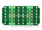
FR4 PCB Multilayer Boards ENIG High Frequency High Level Bonding Material
Quotation Requirement :
a) Base material
b) Board thickness
c) Copper thickness
d) Surface treatment
e) color of solder mask and silkscreen
f) Quantity
Parameter:
| Max panel size | 508*610mm | |
| Board thickness tolerance | T≥0.8mm±8%.,T<0.8mm±5% | |
| Wall hole copper thickness | >0.025mm(1mil) | |
| Finished hole | 0.2mm-6.3mm | |
| Min line width | 4mil/4mil(0.1/0.1mm) | |
| Min bonding pad space | 0.1mm(4mil) | |
| PTH aperture tolerance | ±0.075mm(3mil) | |
| NPTH aperture tolerance | ±0.05mm(2mil) | |
| Hole site deviation | ±0.05mm(2mil) | |
| Profile tolerance | ±0.10mm(4mil) | |
| Board bend&warp | ≤0.7% | |
| Insulation resistance | >1012Ωnormal | |
| Through-hole resistance | <300Ωnormal | |
| Electric strength | >1.3kv/mm | |
| Current breakdown | 10A | |
| Peel strength | 1.4N/mm | |
| Soldmask regidity | >6H | |
| Thermal stress | 28820Sec | |
| Testing voltage | 50-300V | |
| Min buried blind via | 0.2mm(8mil) | |
| Outer copper thickness | 1oz-5oz | |
| Inner cooper thickness | 1/2 oz-4oz | |
| Aspect ratio | 8:1 | |
| SMT min green oil width | 0.08mm | |
| Min green oil open window | 0.05mm | |
| Insulation layer thickless | 0.075mm-5mm | |
| Taphole aperture | 0.2mm-0.6mm | |
| Special technology | Indepedance,Blind buried via,thick gold,aluminum PCB | |
| Surface finish | HASL,Lead free HASL,Immersion Gold, Immersion Tin, Immersion Silver,OSP ,ENIG ,Golden finger,Blue glue,Gold plating | |
Delivery Time for PCB board:
1) PCB production time: sample: 3-4 days / mass production: within 7 days
2) Component purchase: 2 days if all components is available in our domestic market.
3) PCB Assembly: samples: whthin 2 days / mass production: within 5 days
Shipping Method and Payment terms:
1. By DHL, UPS, FedEx, TNT using clients account.
2. We suggest you using our DHL, UPS, FedEx, TNT forwarder.
3. By EMS (Usually for Russia Clients), price is high.
4. By sea for mass quantity according to customer's requirement.
5. By customer's Forwarder
6.By Paypal,T/T,West Union,etc.
Testing Procedures For PCB Board:
We perform multiple quality assuring procedures before shipping out any PCB board.
These include:
* Visual Inspection
* Flying probe
* Impedance control
* Solder-ability detection
* Digital metallograghic microscope
* AOI (Automated Optical Inspection)


