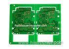
Heavy Copper Plating Double Sided PCB With Customized Technology Requirements
Product type:
Single-sided, double-sided and multilayer printed circuit boards (PCB), flexible (soft) of circuit boards, blind buried plate.
Max size: single-sided, double-sided: 1000mm * 600mm MLB: 600mm * 600mm
Highest Number of floors: 20 floors
Processing board thickness: 0.4mm -4.0mm rigid plate flexible plate 0.025mm --- 0.15mm
Copper foil substrate thickness: rigid plate 18μ (1 / 2OZ), 35μ (1OZ), 70μ (2OZ) flexible board 0.009MM 0.018mm 0.035mm 0.070mm 0.010mm
Common substrates: FR-4, CEM-3, CEM-1, 94HB, 94VO, poly vinyl chloride, polyester, polyimide ammonium.
Process Capability:
(1) Drilling: Minimum aperture 0.15MM
(2) metal hole: Minimum aperture 0.15mm, thickness / aperture ratio of 4: 1
(3) wire width: Minimum width: gold plate 0.075mm, 0.10mm tin plate
(4) lead spacing: Minimum spacing: gold plate 0.075mm, 0.10mm tin plate
(5) gold plate: Ni layer thickness:> or = 2.5μ gold layer thickness: 0.05-0.1μm or according to customer requirements
(6) HASL: tin layer thickness:> or = 2.5-5μ
(7) paneling: Wire-to-edge minimum distance: 0.15mm hole to edge minimum distance: 0.2mm Minimum Shape tolerance: ± 0.12mm
(8) outlet chamfer: angle: 30 degrees, 45 degrees, 60 degrees Depth: 1 -3mm
(9) V cut: angle: 30 degrees, 35 degrees, 45 degrees Depth: 2/3 thickness minimum size: 80mm * 80mm
(10) off test:
Resistance to soldering heat: 85 --- 105 / 280 --- 360
Flexible sheet resistance flexing resistance / chemical resistance: full compliance with international standards
Inspection:
1. The main inspection hole metallization quality status, should ensure that the hole was no extra burr, black holes, holes and so on;
2. Check the substrate surface dirt and other unwanted objects;
3. Check the board number, drawing number, process documentation and process description;
4. clarify racking parts, racking requirements and can withstand the plating tank plating area;
5. plating area, the process parameters to be clear, to ensure the stability and viability of the electroplating process parameters;
6. conductive parts cleaning and preparation, the solution was presented first energization process active;
7. finds bath composition is checked, plate surface area status; such as the use of spherical anode bar installed, you must also check the consumption;
8. Check the voltage solid case and the contact area, the current fluctuation range.


