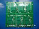
Double Sided Fr4 High Tg 170 PCB 1.6mm Immersion Gold Green For GPS Logger
PCB properties
| PCB SIZE | 191 x 182mm=6PCS |
| BOARD TYPE | |
| Number of Layers | Double sided PCB, 2 Layer PCB |
| Surface Mount Components | YES |
| Through Hole Components | YES |
| LAYER STACKUP | copper ------- 35um(1oz)+plate TOP layer |
| FR-4 1.5mm | |
| copper ------- 35um(1oz)+plate BOT Layer | |
| TECHNOLOGY | |
| Minimum Trace and Space: | 7.8mil/7.4mil |
| Minmum / Maximum Holes: | 0.75/3.0mm |
| Number of Different Holes: | 7 |
| Number of Drill Holes: | 356 |
| Number of Milled Slots: | 0 |
| Number of Internal Cutouts: | 0 |
| Impedance Control | no |
| BOARD MATERIAL | |
| Glass Epoxy: | FR-4, ITEQ IT-180 TG>170, er<5.4 |
| Final foil external: | 1.5oz |
| Final foil internal: | 0oz |
| Final height of PCB: | 1.6mm ±0.16 |
| PLATING AND COATING | |
| Surface Finish | Immersion Gold (13.4%) 2micoinch over 100 microinch nickle |
| Solder Mask Apply To: | Top and Bottom, 12micron Minimum |
| Solder Mask Color: | Gloss Green, Taiyo PSR-2000GT600D |
| Solder Mask Type: | LPSM |
| CONTOUR/CUTTING | Routing, Fiducial Marks |
| MARKING | |
| Side of Component Legend | TOP |
| Colour of Component Legend | White, IJR-4000 MW300, Taiyo Supplied. |
| Manufacturer Name or Logo: | Marked on the board in a conductor and leged FREE AREA |
| VIA | Plated Through Hole(PTH), via tented |
| FLAMIBILITY RATING | UL 94-V0 Approval MIN. |
| DIMENSION TOLERANCE | |
| Outline dimension: | 0.0059" |
| Board plating: | 0.0029" |
| Drill tolerance: | 0.002" |
| TEST | 100% Electrical Test prior shipment |
| APPLICATION: | GPS logger |
| TYPE OF ARTWORK TO BE SUPPLIED | email file, Gerber RS-274-X, PCBDOC etc |
| SERVICE AREA | Worldwide, Globally. |
Advantages
a) High Tg substrate. Excellent thermal reliability and CAF resistance providing long-term reliability for industrial and automobile application.
b) Electroless nickel immersion gold. Long storage time ( It can be stored for more than 1 year in vacuum bag)
c) Eligible products rate of first production: >95%
d) Devlivery on time: >98%
More Applications in Electronics
Wireless Router
Hdmi
Navigation
Modem
Speaker
Switched Mode Power Supplies
Contract Electronics Manufacturing
High Power Supply
Electronics Manufacturing Service
Power Supply Output
PCB knowlege: PCB classification
Classification by layers: It's divided into a single sided PCB, double sided PCB and multilayer PCB. The Common multilayer board is generally 4 layers or 6 layers, complex multilayer board up to dozens of layers.
Single Sided PCB
Single Sided Boards are the most basic parts of PCB. Components are concentrated on one side, the wire track is focused on the other side (SMD components and wires for the same side, then the other side of the through-hole components). Because the wire appears only in one side, so this kind of PCB is called single sided.
It has many strict restrictions in the design on the line (because of only one side, each wire must not cross and goes around its own path), so this type of circuit board is used at the early stage of circuit.
Double sided PCB
Both sides of the circuit board are wired, but to use the two sides of the wire, we must have the proper circuit connection between the two sides. The "bridge" between the circuits is called the pilot hole (via). The via is filled with or coated with a small hole in the PCB. It can be connected to the two sides of the wire. Because double sided PCB is twice larger in area than a single sided PCB, it solves the difficulty that wiring staggered in single side PCB (through hole conduction to the other side). It is more suitable for use in circuits that are more complex than a single sided board.
Multilayer PCB
In order to increase the area that can be wired, multilayer board uses more single or double sided wiring board.
PCB using a double side board as inner layer and two pieces of single layer as the outer layer or two double-sided printed circuit board as the inner layer and two pieces of single layer as the outer layer, through the insulation and bonding materials to press each layer together, and the conductive pattern are as per design requirements for interconnection becomes the 4 layers of printed circuit board, 6 layers of printed circuit board, also known as multilayer printed circuit board.
The number of layers of the board does not represent a separate layer of wiring. In particular, the air layer will be joined to control the thickness of the board. Usually the number of layers is even, and contains the outermost 2 layers. Most of the host mainboard is 4 to 8 layers of structure, but the theory can be technically nearly 100 layers of PCB boards. Large supercomputers use quite a lot of layers of mainframe board, but because this kind of computer can be replaced with a lot of ordinary computer clusters, super multilayer board has gradually not been used. Because all of the layers in the PCB are closely combined, it is generally not easy to see the actual number, but if you look carefully at the motherboard, you can also see it.
PCB can be also classified by its softness. There’re rigid PCB, flexible PCB and Rigid-flex PCB. Metal core PCB and high frequency PCB are classified by its material.
FAQ
How do you pack the PCBs?
PCBs are packed with Polyethylene air cushion film(vacuum plastic bags) per 20-25 pieces. Pearl cotton (Polyethylene foamed sheet) are put inside carton box.
The hardness of carton box is KK grade(the highest hardness). Maximum gross weight for one carton is less than 12 kgs.