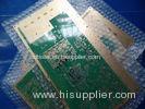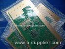


10 Layer High Frequency PCB Design RO4350B Core For Broadband Wireless Solutions
PCB properties
| PCB SIZE | 215 x 178mm=1PCS=1design |
| BOARD TYPE | |
| Number of Layers | Multilayer High Frequency PCB, 10 Layer PCB |
| Surface Mount Components | YES |
| Through Hole Components | NO |
| LAYER STACKUP | TOP Layer: signal - 1/2oz foil + 25μm Cu |
| Core RO4350B -0.254mm | |
| INT 1: mixed - 1/2oz foil | |
| Prepreg RO4450B -0.202mm (2 x 0.101) | |
| INT 2: mixed - 1/2oz foil | |
| Core RO4350B -0.254mm | |
| INT 3: mixed - 1/2oz foil | |
| Prepreg RO4450B -0.202mm (2 x 0.101) | |
| INT 4: mixed - 1/2oz foil | |
| Core RO4350B -0.254mm | |
| INT 5: mixed - 1/2oz foil | |
| Prepreg RO4450B -0.202mm (2 x 0.101) | |
| INT 6: mixed - 1/2oz foil | |
| Core RO4350B -0.254mm | |
| INT 7: mixed - 1/2oz foil | |
| Prepreg RO4450B -0.202mm (2 x 0.101) | |
| INT 8: mixed - 1/2oz foil | |
| Core RO4350B -0.254mm | |
| BOT Layer: signal - 1/2oz foil + 25μm Cu | |
| TECHNOLOGY | |
| Minimum Trace and Space: | 5.5mil/5mil |
| Minmum / Maximum Holes: | 0.3/2.0mm |
| Number of Different Holes: | 9 |
| Number of Drill Holes: | 7505 |
| Number of Milled Slots: | 0 |
| Number of Internal Cutouts: | 0 |
| Impedance Control | NO |
| BOARD MATERIAL | |
| Glass Epoxy: | RO4350B core 0.254mm(10mil), RO4450B PP 0.1mm(4mil) |
| Final foil external: | 1oz |
| Final foil internal: | 0.5oz |
| Final height of PCB: | 2.0mm ±10% |
| PLATING AND COATING | |
| Surface Finish | Electroless Nickle over Immersion Gold (ENIG)( 0.05µm over 3µm nickle) |
| Solder Mask Apply To: | Top and Bottom, 12micon Minimum. |
| Solder Mask Color: | Green, PSR-2000GT600D, Taiyo supplied. |
| Solder Mask Type: | LPSM |
| CONTOUR/CUTTING | Routing |
| MARKING | |
| Side of Component Legend | TOP |
| Colour of Component Legend | White, IJR-4000 MW300, Taiyo Supplied. |
| Manufacturer Name or Logo: | Marked on the board in a conductor and leged FREE AREA |
| VIA | Plated Through Hole(PTH), via tented. BGA package |
| FLAMIBILITY RATING | UL 94-V0 Approval MIN. |
| DIMENSION TOLERANCE | |
| Outline dimension: | 0.0059" (0.15mm) |
| Board plating: | 0.0030" (0.076mm) |
| Drill tolerance: | 0.002" (0.05mm) |
| TEST | 100% Electrical Test prior shipment |
| APPLICATION: | Broadband wireless solutions |
| TYPE OF ARTWORK TO BE SUPPLIED | email file, Gerber RS-274-X, PCBDOC etc |
| SERVICE AREA | Worldwide, Globally. |
Advantages
a) RO4350B substrate. Excellent high frequency performance due to low dielectric tolerance and loss.
b) Stable electrical coefficient of dielectric constant.
c) Excellent dimensional stability.
d) Excellent surface planarity, particularly helpful for PCBs with BGA packages or even CSP mounted components to reduce failure rate during assembly and soldering.
e) Good oxidation resistance and good heat dissipation.
f) No MOQ, low cost for small quantity prototypes and samples.
More Applications in Electronics
Wifi Usb Dongle
Modem Router Wireless
Gsm Tracker
Antena Wireless
Bluetooth
Multiplexer
Gps Antenna
Satellite Antenna
Tv Antenna
Combiner
Design for Manufacture (1)
| Serial NO. | Procedure | Item | Manufacturing capability | ||
| Large volume (S<100 m²) | Middle volume (S<10 m²) | Prototype(S<1m²) | |||
| 1 | Inner layer (18um, 35um, 70um etc are finished copper. If not mentioned copper, finished 1oz is the default value ) | Min.isolation of layers | 0.1mm | 0.1mm | 0.06mm |
| 2 | Min.track and spacing | 5/5mil(18um) | 4/4mil(18um) | 3/3.5mil(18um) | |
| 3 | 5/5mil(35um) | 4/4mil(35um) | 3/4mil(35um) | ||
| 4 | 7/9mil(70um) | 6/8mil(70um) | 6/7mil(70um) | ||
| 5 | 9/11mil(105um) | 8/10mil(105um)
Didn't find what you're looking for?
Post Buying Lead or
contact our customer service specialist for help!
About HiSupplierUser GuideFeatured Partners:
Follow Us:


Channel: madeinchina.hisupplier.com - hebei.hisupplier.com - ningbo.hisupplier.com Language Option: العربية - Nederlands- Français- Deutsch- Italiano- 日本語- 한국의- Português- Pусский- Español IPR Protection Policy - Terms of Use - Privacy Policy - Security Measures Copyright © HiSupplier.com Online Inc. All Rights Reserved. 
| |||