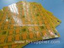
Multilayer Via In Pad PCB FR4 0.5 Mm Yellow GPS Antenna PCB Design
PCB parameters
| PCB SIZE | 102 x 100mm=81PCS |
| BOARD TYPE | |
| Number of Layers | Multilayer, 4 layer PCB |
| Surface Mount Components | YES |
| Through Hole Components | NO |
| LAYER STACKUP | copper ------- 18um(0.5oz)+plate TOP |
| 4mil prepreg | |
| copper ------- 18um(0.5oz) GND | |
| 4mil FR-4 | |
| copper ------- 18um(0.5oz) PWR | |
| 4mil prepreg | |
| copper ------- 18um(0.5oz) | |
| TECHNOLOGY | |
| Minimum Trace and Space: | 3mil/4mil |
| Minmum / Maximum Holes: | 0.25/4.50mm |
| Number of Different Holes: | 21 |
| Number of Drill Holes: | 503 |
| Number of Milled Slots: | 0 |
| Number of Internal Cutouts: | 0 |
| Impedance Control | no |
| BOARD MATERIAL | |
| Glass Epoxy: | FR-4, ITEQ IT140 TG>135, er<5.4 |
| Final foil external: | 1oz |
| Final foil internal: | 0.5oz |
| Final height of PCB: | 0.5mm ±0.1 |
| PLATING AND COATING | |
| Surface Finish | Immersion gold 0.05µm over 3µm Nickel, (11.7% area) |
| Solder Mask Apply To: | TOP and Bottom, 12micron Minimum |
| Solder Mask Color: | Yellow, Taiyo PSR-2000GT600D |
| Solder Mask Type: | LPSM |
| CONTOUR/CUTTING | Routing |
| MARKING | |
| Side of Component Legend | No silkscreen requried. |
| Colour of Component Legend | No silkscreen requried. |
| Manufacturer Name or Logo: | No silkscreen requried. |
| VIA | Plated through hole(PTH), Via in Pad. |
| FLAMIBILITY RATING | UL 94-V0 Approval MIN. |
| DIMENSION TOLERANCE | |
| Outline dimension: | 0.0059" (0.15mm) |
| Board plating: | 0.0030" (0.076mm) |
| Drill tolerance: | 0.002" (0.05mm) |
| TEST | 100% Electrical Test prior shipment |
| APPLICATION: | Antenna |
| TYPE OF ARTWORK TO BE SUPPLIED | email file, Gerber RS-274-X, PCBDOC etc |
| SERVICE AREA | Worldwide, Globally. |
Advantages
a) UL94V0 flame retardant. Thin laminates and thin Prepreg for multilayer PCB
b) Immersion gold PCB. Good oxidation resistance and good heat dissipation.
c) 100% tests inclusive of electrical test and AOI inspection.High voltage test, Impedance control test, micro-section, solder-ability test, thermal stress test, reliability test, insulation resistance test and ionic contamination test etc.
d) Meeting your printed circuit board needs from PCB prototyping to mass volume production.
More Applications in Electronics
Wifi Booster
HDMI Switch
Voip
Remote Control
Oscilloscope
Design for Manufacture (3)
| Serial NO. | Procedure | Item | Manufacturing capability | ||
| Large volume (S<100 m²) | Middle volume (S<10 m²) | Prototype(S<1m²) | |||
| 35 | Solder mask (18um, 35um, 70um etc are finished copper. If not mentioned copper, finished 1oz is the default value ) | Maximum via-plug diameter | 0.5mm | 0.5mm | 0.5mm |
| 36 | Min.width of solder mask bridge | Green:5mil(35um) | Green:4mil(35um) | Green:4mil(35um) | |
| 37 | Yellow:5mil(35um) | Yellow:4mil(35um) | Yellow:4mil(35um) | ||
| 38 | Blue:5mil(35um) | Blue:4mil(35um) | Blue:4mil(35um) | ||
| 39 | Black:6mil(35um) | Black:6mil(35um) | Black:6mil(35um) | ||
| 40 | White:6mil(35um) | White:6mil(35um) | White:6mil(35um) | ||
| 41 | All of Matt:6mil | All of Matt:6mil | All of Matt:6mil | ||
| 42 | Green:5mil(70um) | Green:4mil(70um) | Green:4mil(70um) | ||
| 43 | Yellow:5mil(70um) | Yellow:4mil(70um) | Yellow:4mil(70um) | ||
| 44 | Blue:5mil(70um) | Blue:4mil(70um) | Blue:4mil(70um) | ||
| 45 | Black:6mil(70um) | ||||