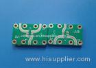


Antenna Green 2 Layer RF PCB 30mil 1 Oz High Frequency Circuit Design
PCB properties
| PCB SIZE | 38 x 25mm=1PCS |
| BOARD TYPE | |
| Number of Layers | Double sided PCB |
| Surface Mount Components | YES |
| Through Hole Components | NO |
| LAYER STACKUP | copper ------- 35um(1oz)+plate TOP layer |
| RO4350B 30mil (0.762mm) | |
| copper ------- 35um(1oz)+plate BOT Layer | |
| TECHNOLOGY | |
| Minimum Trace and Space: | 78mil/30mil |
| Minmum / Maximum Holes: | 0.8/3.5mm |
| Number of Different Holes: | 2 |
| Number of Drill Holes: | 53 |
| Number of Milled Slots: | 0 |
| Number of Internal Cutouts: | 0 |
| Impedance Control | NO |
| BOARD MATERIAL | |
| Glass Epoxy: | RO4350B 30mil (0.762mm), Tg 288 |
| Final foil external: | 1.5oz |
| Final foil internal: | 0oz |
| Final height of PCB: | 0.8mm ±0.1 |
| PLATING AND COATING | |
| Surface Finish | Electroless Nickle over Immersion Gold (ENIG)( 1 µ" over 100 µ" nickle) |
| Solder Mask Apply To: | Top,12micon Minimum. |
| Solder Mask Color: | Green, PSR-2000GT600D, Taiyo supplied. |
| Solder Mask Type: | LPSM |
| CONTOUR/CUTTING | Routing |
| MARKING | |
| Side of Component Legend | TOP |
| Colour of Component Legend | White, IJR-4000 MW300, Taiyo Supplied. |
| Manufacturer Name or Logo: | Marked on the board in a conductor and leged FREE AREA |
| VIA | Plated Through Hole(PTH), Via tented |
| FLAMIBILITY RATING | UL 94-V0 Approval MIN. |
| DIMENSION TOLERANCE | |
| Outline dimension: | 0.0059" (0.15mm) |
| Board plating: | 0.0030" (0.076mm) |
| Drill tolerance: | 0.002" (0.05mm) |
| TEST | 100% Electrical Test prior shipment |
| APPLICATION: | Antenna |
| TYPE OF ARTWORK TO BE SUPPLIED | email file, Gerber RS-274-X, PCBDOC etc |
| SERVICE AREA | Worldwide, Globally. |
Advantages
a) Lower temperature coefficient of dielectric constant .
b) Ideal for temperature sensitive applications.
c) Devlivery on time: >98%
d) Customer complaint rate: <1%
More Applications in Electronics
Router Antenna
Solar Power Inverter
Electric Converter
Computer Router
Solar Inverters
PCB knowledge: The process of multilayer PCB
A) In general, a multilayer board consists of a number of very thin print-and-etch inner layers, but drilling of holes has not been carried out. Outer layers of the multilayer board remain unetched.
B) Layers from top to bottom are bonded together in close registration by means of thin plies of prepreg. The bonding is performed under close temperature and pressure control in a lamination press.
C) After lamination, they are the processed in very much the same way as an ordinary double-sided PTH boards, i.e. holes are drilled, cleaned and plated. Outer layers are etched to develop the circuit pattern. Solder masks are applied and solder coating (HAS, ENIG etc) is performed.

Microsection, FR-4, 12 layers
FAQ
Do you sell cheap FR-1, CEM-1 PCB?
Yes, we just offer single sided PCB made of FR-1 and CEM-1. We also use punching tool for the contour for the mass production.


