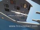


White High Tg 170 1.6mm HASL Lead Free PCB Assembly Services For PLC Control
PCB parameters
| PCB SIZE | 93.5 x 87.1mm=6PCS |
| BOARD TYPE | |
| Number of Layers | Double Sided PCB, 2 layer PCB |
| Surface Mount Components | YES |
| Through Hole Components | NO |
| LAYER STACKUP | copper ------- 18um(0.5 oz)+plate TOP layer |
| FR-4 1.5mm | |
| copper ------- 18um(0.5 oz)+plate BOT Layer | |
| TECHNOLOGY | |
| Minimum Trace and Space: | 5.6mil/4.4mil |
| Minmum / Maximum Holes: | 0.4/4.3mm |
| Number of Different Holes: | 12 |
| Number of Drill Holes: | 831 |
| Number of Milled Slots: | 15 |
| Number of Internal Cutouts: | 1 |
| Impedance Control: | no |
| Number of Gold finger: | 0 |
| BOARD MATERIAL | |
| Glass Epoxy: | FR-4, ITEQ IT-180 TG>170, er<5.4 |
| Final foil external: | 1oz |
| Final foil internal: | 0oz |
| Final height of PCB: | 1.6mm ±0.16 |
| PLATING AND COATING | |
| Surface Finish | Hot Air Soldering Leveling(HASL), Sn>=2.54µm |
| Solder Mask Apply To: | TOP and Bottom, 12micron Minimum |
| Solder Mask Color: | White, PSR400 WT02, Taiyo Supplied |
| Solder Mask Type: | LPSM |
| CONTOUR/CUTTING | Routing |
| MARKING | |
| Side of Component Legend | TOP |
| Colour of Component Legend | Black |
| Manufacturer Name or Logo: | Marked on the board in a conductor and leged FREE AREA |
| VIA | Plated through hole(PTH), via tented. |
| FLAMIBILITY RATING | UL 94-V0 Approval MIN. |
| DIMENSION TOLERANCE | |
| Outline dimension: | 0.0059" (0.15mm) |
| Board plating: | 0.0030" (0.076mm) |
| Drill tolerance: | 0.002" (0.05mm) |
| TEST | 100% Electrical Test prior shipment |
| APPLICATION: | Plc Control |
| TYPE OF ARTWORK TO BE SUPPLIED | email file, Gerber RS-274-X, PCBDOC etc |
| SERVICE AREA | Worldwide, Globally. |
Advantages
a) High Tg170 FR-4. UL94V0. Lead-Free Assembly Compatible, RoHS compliant and suitable for high thermal reliability needs, and Lead free assemblies with a maximum reflow temperature of 260
b) Double sided HASL PCB. Excellent wetting during component soldering and it can avoid copper corrosion.
c) 100% tests inclusive of electrical test and AOI inspection.High voltage test, Impedance control test, micro-section, solder-ability test, thermal stress test, reliability test, insulation resistance test and ionic contamination test etc.
d) Delivery on time. We keep higher than 95% on-time-delivery rate.
More Applications in Electronics
Embedded Systems Programming
Led Lighting Systems
Embedded Systems Basics
Embedded Web Server
Cheap Gps Tracker
PCB knowledge: PCB Production Process
1. Contact PCB fabricator
Contact your satisfied vendor such as Bicheng. You’re registered and will be quoted for you. Place your order and follow up the production schedule.
2. Material cutting
Purpose: According to the requirement from engineering data, cut the large plate which is in compliance with the requirement into small pieces of production board piece to meet customer requirements of the small sheet.
3. Drill
Purpose: According to the requirement from engineering data, drill all the holes.
4. Copper deposition
Purpose: Copper deposition is a thin copper deposit on the wall of the insulating hole by chemical method
5. Pattern transfer
Purpose: Pattern transfer is the transfer of image production on the film to the board
6. Pattern plating
Purpose: Pattern electroplating is a layer of copper or gold over nickel or tin that requires a thickness plated on the exposed copper of the pattern graphic or on the hole wall.
7. Film stripping
Purpose: The NaOH solution is used to strip the anti-plating film to expose the non-pattern circuit layer.
8. Etching
Purpose: Etching is to etch off the non-circuit parts of the copper layer by chemical reaction method
9. Solder Mask
Purpose: Solder mask is transferring the solder mask film graphics to the board to protect the track and prevent the track from the effect of tin welding during assembly.
10. Silkscreen
Purpose: The silkscreen character is a mark that is easy to recognize.
11. Edge connector plating (Gold finger)
Purpose: A nickel gold layer with a thickness is plated on the PCB edge of the plug to make it more resistant to wear.
HASL (a process of coordinate)
HASL is a layer of tin generated on the non-solder mask area to protect pad copper surface from oxidation to ensure good welding performance.
12. Contour
Purpose: By stamping or milling machine to cut the PCB into customers' required shape.
13. Electrical test
Purpose: Through the electronic 100% test to find the open circuit, short circuit and other functional defects which are not easy to find by visual inspection.
14. Final Inspection
Purpose: Through 100% visual inspection to find out the defects in appearance and repair minor defects to avoid problems and defects in the shipment.

FAQ
Do you sell flexible PCB(FPC)?
Yes, we offer flexible printed c


